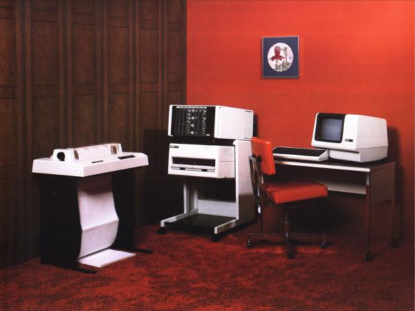
A MINC-11 set in a typical Dec laboratory setting
This describes the Minc-11
A MINC-11 set in a typical Dec laboratory setting
The MINC-11 system is basically a PDP-11/03 (later 11/23) but designed for laboratory use, as a succesor of the LINC system. It used a special set of interface modules and double spaced quad sized slots. The operating system is a special version if RT-11 which launces direct into MINC-Basic. Special functions address the MINC modules and graphic capabilities of the VT-105 terminal. The modules are:
Connecting the modules to the real world was sometimes done with BNC-connectors at the module front, but mainly via the connector block on top of the modules. The C/D connectors of the QBus are used to connect modules, like a preamplifier and/or multiplexer as A/D converter front end.
MINC Basic also supported instrument interfacing via serial and IEEE bus, but used conventional QBus cards for this (DLV11-J resp. IBV11)
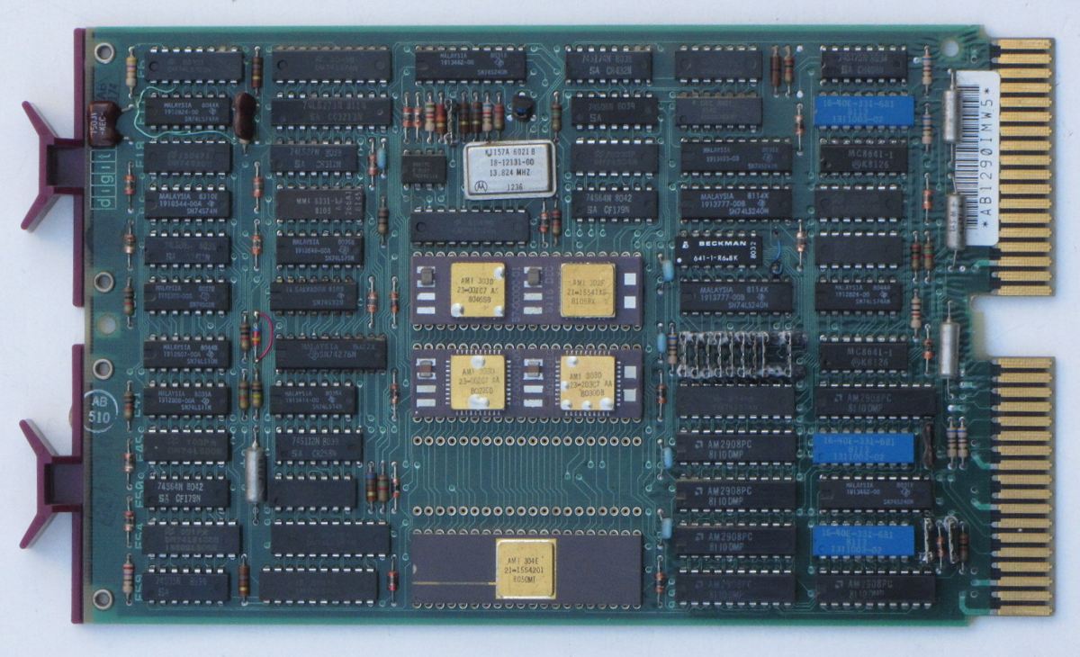
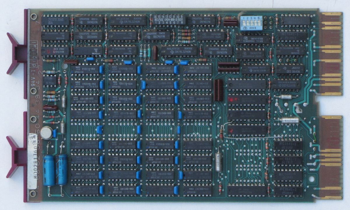
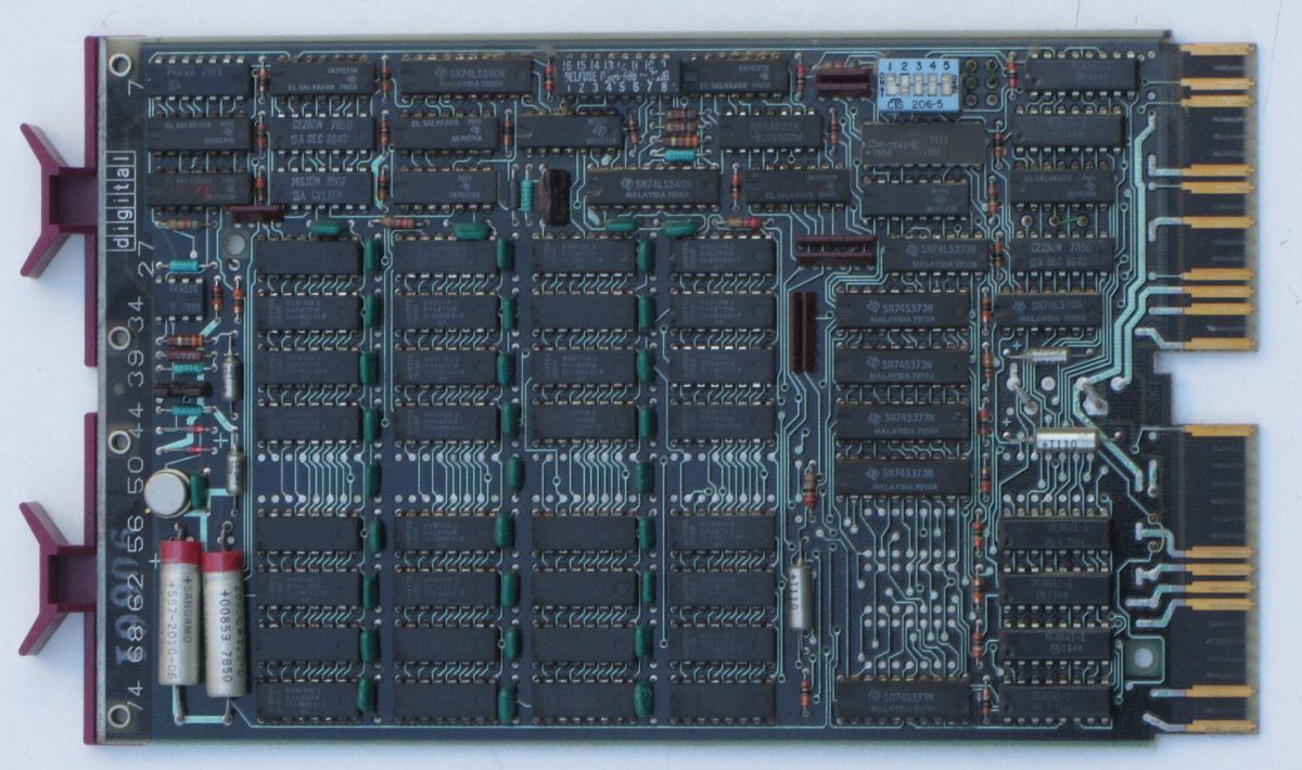
This are the boards in my Minc-11, with info from the various DEC documents, I think useful and/or interesting.
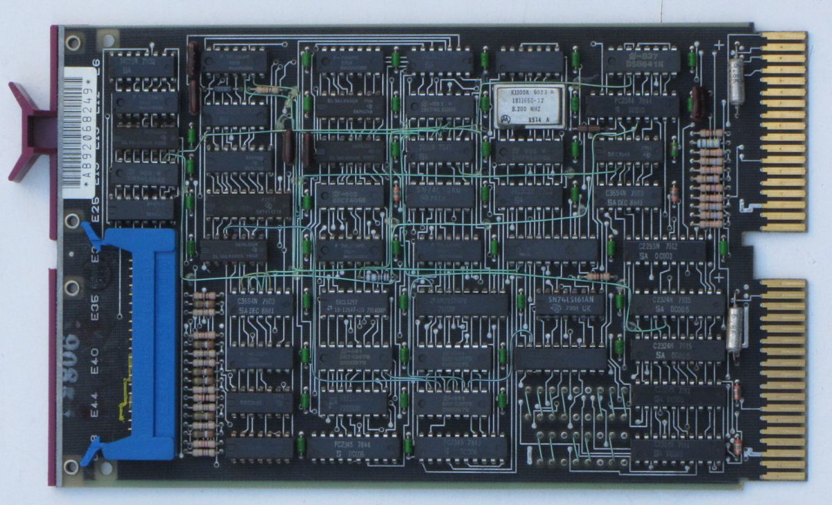
| KDF11-AA M8186 |
|
This board has the F-11 chipset:
Found the I/O page at 770000 - 777777, so this is an 18-bit machine. Note this is in ODT mode, it is 177000 - 177777 when a program is executed. So ODT bypasses the MMU. |
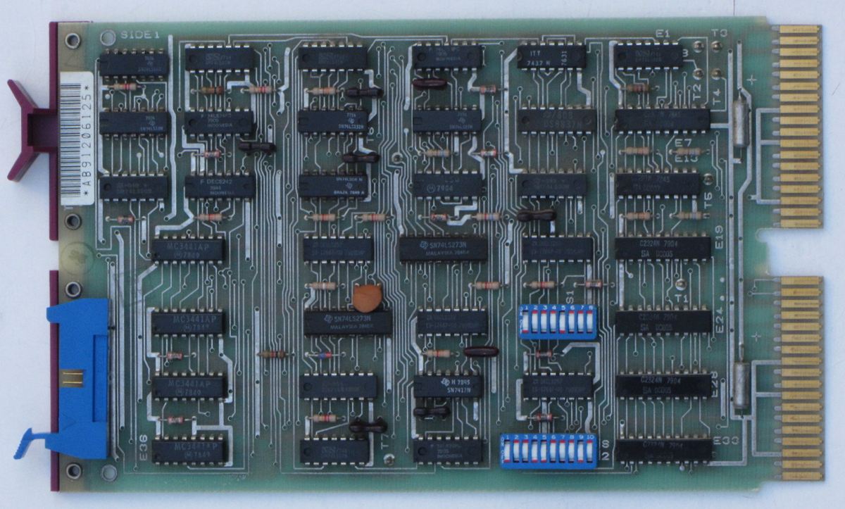
| MSV11-DD M8044 DH |
|
32 kW with Nec UPD416. The -5V required by the RAM chips is generated on board. Dynamic RAM refresh is also local. There is no parity bit on this board (MSV11-E only). |
| MSV11-DD M8044 DB |
|
32 kW with Mostek MK4116. The -5V required by the RAM chips is generated on board. Dynamic RAM refresh is also local. There is no parity bit on this board (MSV11-E only). |
| RXV21 M8029 |
|
RX02 floppy interface. These are the commands
Like with the RX01 interface, there is no way to format a floppy disk. As the format is unique for DEC, the only way to get an usable floppy is buying them from DEC. But it is possible to 'convert' a RX01 (standard IBM single density) to RX02. (RX02 is a single density sector header combined with double density data) Booting from an RX01 or RX02 floppy means the bootstrap loader program has to be loaded first from the REV11-A or BVD11 option. |
| IBV11-A M7954 |
|
IEEE-488 interface. The IEEE-488 bus is widely used in laboratory environments, so this interface is very useful for a Minc. |
| ? G7272 |

|
The LSI11 GRANT CONTINUITY shorts AM2(BIAKI) with AN2(BIAKO), and
AR2(BDMGI) with AS2(BDMGO). This configuration is not unique to the
LSI11 GRANT CONTINUITY, all cards that do not use DMA or interrupts have
these shorts. BIAKI = Interrupt acknowledge input, BIAKO = Interrupt acknowledge output. BDMGI = DMA Grant Input, BDMGO = DMA Grant Output. These connection allows unused slots between the processor and DMA and interrupt cards. Without this board, the DMA and interrupt chain would not work. |
| DLV11-J M8043 |
|
The four-channel serial interface. The 10 pin header on the board is
connected to 9-pin DE-9 male connectors on the chassis. This ASCII art
shows the connection and a cable to a standard PC serial port.
     DLV11-J 10 pin header    chassis 9-pin DE-9     EIA RS-232C DB-25 (25p.) female [DE-9 (9p.)]
      1 - 16x Baud rate -------- 1 --:-
      2 - GND ------------------ 3 --:- )----------------------( GND 7       [5]
      3 - XMIT DATA + ---------- 4 --:- )----------------------( RCV DATA 3  [2]
      4 - XMIT DATA - ---------- 5 --:-
      5 - GND ------------------ 9 --:-
      6 - slot
      8 - RCV DATA + ----------- 7 --:- )----------------------( XMIT DATA 2 [3]
      7 - RCV DATA - ----------- 8 --:- )--+
                                           |
      9 - GND ------------------ 6 --:- )--+
     10 - +12V ----------------- 2 --:-
For a real PC DB-25 also connect pin 4 with 5, and 6 with 8 and 20. For 9-pin DE-9: 7 with 8, and 1 with 4 and 6
|
| BDV11 M8012 |
|
The LEDs on the board might be useful during startup when there is no prompt
or other feedback, but as they are operated by software only, nothing happens
in the critical phase. Most useful is the green LED indicating the
bus voltages ar more or less ok.
S1 (Halt/Normal switch) / = processor in run mode; \ = processor in halt mode; (single instruction) S2 (Boot/Normal switch) toggle is restart There are lots of sockets and switches on the board, so how does it work?
|
| MNCAD |
|
Analog-digital converter module |
| MNCAA |
|
Digital-analog converter module |
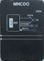
| MNCD0 |
|
Digital out module |
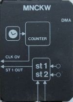
| MNCKW |
|
Clock module |
| Module order |


|
The diagrams on top of the modules indicate that the MNCAD depends on a MNCKW in the slot right of it. One or more digital options in between are allowed as these pass the clock through the clock signals. If you want another analog-digital module, you also need a second clock module. |
The MP01074_MDL-23_MINC_Engineering_Drawings_Jun80.pdf document at bitsavers.org contains much info on the Minc-23 system.
Local links:
Generic links:
Last update: 2021-01-09